Agat-7. Rev.0. CPU, memory and joystics
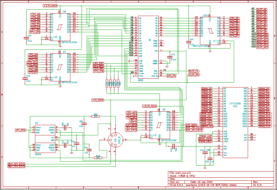
Let’s go to the following part of the schematic. Today it is the CPU, the SRAM and the joysticks. Here it is:
“Agat-7” has 96Kb of RAM, so we need a 128Kb SRAM chip. We can use 128K x 8bit or 64K x 16bit chips. The second option requires connecting nine more FPGA pins, which suits our needs. The 1024х768х65Hz output involves a lot of data to be read from SRAM between CPU use of the bus. It is possible to reach it with 10ns SRAM by transmitting 2 bytes for each cycle which is achievable with the second type of SRAM.
CE and OE inputs can be tied to the ground because we will not use them.
6502 CPU requires a 5V power supply, and its output that I’ve measured is 4.1V, which is a bit high for FPGA. I used SN74LVC245A buffers to shift levels. They are pretty cheap – about $0.25 in retail. The direction of the level shift is switched by the R/W output of the CPU for the data bus, tied to the ground for the rest, and fixed in the direction from CPU to FPGA. Signals from FPGA have a 3.2V level and can be used as is. One of the buffers has some spare pins, which I’ve used for other 5V parts of the computer, i.e. a keyboard and joystick.
The Joystick circuit is also located on this sheet. In “Agat-7”, it was done with a timer KR1006VI1, which is the Soviet analog of the popular NE555 chip. It connects as a monostable multivibrator, and an output pulse length depends on the position of a potentiometer in the joystick. The computer measures the length and determines the position. The same idea was used in the “Apple ][” computer, and I can assume it was copied from there.
For compatibility, I use the same circuit in my design. To cut some price and save some PCB space, I use the NE556 chip, which consists of two NE555 in one case.
The request pulse comes straight from FPGA. The output pulse goes from the level shifter chip, which is unnecessary because according to the datasheet NE556 output level will be about 2.4V.
Joystick buttons are connected to a level shifter as well.
SLOT output is connected to the extension slot on the board.
That’s all for today. Please, let me know if you discover any mistakes in the design. Stay tuned!
